


INTRODUCTION
More oscillator odds and ends. These aren't complete projects, just bits of tinkering and trying
things out but they may be of interest for all that.
This one started out as playing with the simulator. The circuit itself came from an old
applications manual published in the 1970s by Ferranti[1] (they later became Zetex and then a
part of Diodes Inc), though the original didn't have the loudspeaker - I added that.
A RAMP GENERATOR
This is a ramp generator and the output signal derives from the charging of a capacitor. Back
then, analogue circuits to generate ramps in various forms were important as they got used for
all sorts of things, including scanning cathode-ray tubes in displays and vidicon tubes in
cameras.
Sometimes ramps are simply triggered by other circuits but by detecting when the ramp reaches a
set point and having a mechanism to discharge the capacitor when that occurs we get an
oscillator. It's essentially the same method used by the unijunction transistor and the 555 timer
circuits which I recently blogged about, so if you compiled a taxonomy of circuits they'd
probably all fall in the same class.
THE CIRCUIT
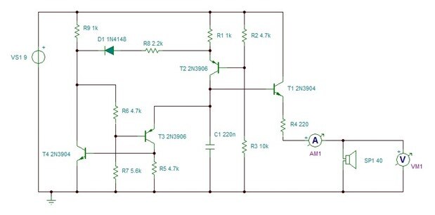
Here's the schematic as I've drawn it in the simulator. The original used ZTX300 and ZTX500
transistors, but I've changed them for 2N3904 and 2N3906 respectively.
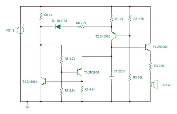
For clarity at this stage, I've left off the measuring components (like test meters) that you'd
normally have attached so that you could see what the circuit was doing under a transient test.
I've also drawn it with the ground wired, rather than implied by using ground symbols all over
the diagram, as that probably makes reading the circuit a bit easier. The circle with the
identifier VS1 and the number 9 against it is a 9V voltage source. It's standing in for a battery
or a PSU. The transistors are low-cost, small-signal parts and aren't at all critical. The
loudspeaker (SP1) has a dc resistance of 40 ohms (simply because I had one - it would work with
an 8 ohm speaker, but would be quieter). I've included one ground symbol to keep the simulator
happy - it likes to know which net is the ground reference point that all the other voltages will
be with respect to.
If you are used to constructing circuits, there should be enough there to take it and make it on
a breadboard - I'm going to do that after I've looked at it in the simulator. As it stands it
oscillates at a single frequency so it would make a very dreary musical instrument. Later I'll
take a look at how the frequency of oscillation could be varied in order to get different notes.
HOW IT WORKS
Because the circuit doesn't have an input and, as it doesn't flow nicely from left to right in
the way that some circuits do, it's slightly confusing to understand at first glance. There's
also the problem that a) there's some feedback at work that's slightly hidden if you're not used
to interpreting what transistor circuits do and b) there's something that looks like it might be
feedback that isn't.
So where do we start? The most obvious place is the capacitor, C1 (particularly as I've already
said that the ramp derives from a capacitor charging). Even if I hadn't given you that clue, it
would still be the natural place to start because it's the only component in the circuit that can
give a significant time delay. Next question, then, is: how does the capacitor charge? You've
probably seen circuits where the current to charge a capacitor comes through a resistor, but that
isn't the case here, instead we are faced with a connection to three transistors, any one of
which could be involved.
The transistor that controls the charging current is T2. How do I know that? Well, the charging
current has to have a path down from the positive supply rail and R1+T2 is the only path that
will satisfy that - the emitter-base diode of T3 is reverse biased against a current flowing down
through R9 and R6, and the collector-base diode is reverse-biased against a current flow that
arrives back through T1. Alternatively, if you were familiar with transistor circuits, you might
just directly recognise the circuit configuration of T2, R1, R2, and R3 as being a current source
that could supply charge to the capacitor.
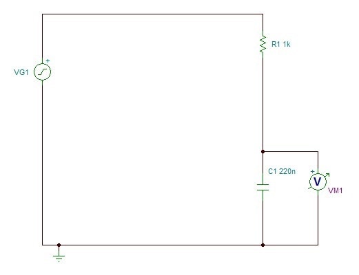
So why all this complication? Why not just charge the capacitor through a resistor?
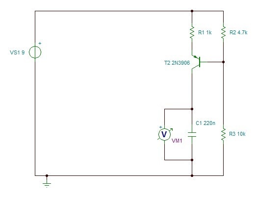
Here's the [simplified] circuit if we just had a resistor. In this circuit I've substituted a
voltage generator for the voltage source. It is set up to simply give a step from 0V to 9V right
at the start (if I use a voltage source, the simulator doesn't properly understand what happens
at the start).
if I do a transient plot of this in the simulator, it comes up with this for the voltage across
the capacitor
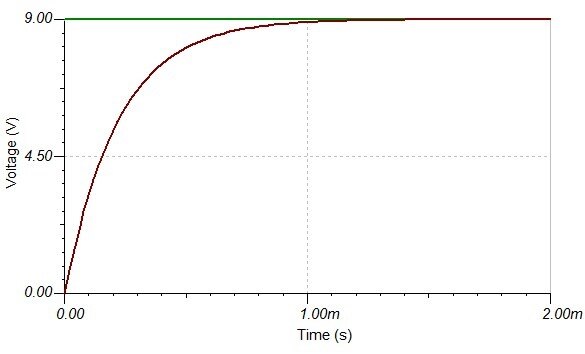
That waveform isn't linear because, as the capacitor charges, the voltage across the resistor
drops and the charging current drops too. To get around that we need a constant current.
In this next circuit, I've isolated T2 and the three resistors associated with it so we can see
how it behaves. The collector I'm driving with a ramp from the voltage generator, VG1, and I'm
measuring the current with AM1 so that we'll see the current we get for different voltages at the
collector.

Here are the traces
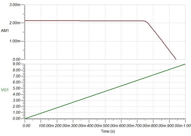
What this shows is that, irrespective of the voltage at the collector, it will maintain the
current at just over 2mA all the way up to about 7.5V.
So, how does it do that? The pair of resistors, R2 and R3, form a potential divider and give a
voltage at the base of the transistor of about 6.2V. The emitter will be 0.6V above that, so say
6.8V. That gives a voltage drop across resistor R1 of 9V - 6.8V = 2.2V and that results in a
current through the resistor of approximately 2.2mA. Most of that current will flow out of the
collector, provided it is lower than about 6.5V.
Now here's what happens if I couple the constant current circuit to the capacitor.
I've included a voltage meter to measure the voltage across the capacitor. The component marked
'IC1 0' isn't a component at all - it's an initial condition and forces that point of the circuit
to 0V at time 0 (and then has no further effect). For some reason that I don't understand, that's
necessary to get the capacitor to start from 0V even though I've set the capacitor start voltage
as 0V in its parameter list.
Here's the waveform and, as we can see, it's now a reasonably linear ramp up to about 7V or so.
So, how does it reset to start a fresh cycle? That's done by T3 and T4. T3 sets the trigger point
and T4 ensures that once the capacitor discharge starts to happen that it's fast and completes.
When the voltage across the capacitor is low T3 is off and, as there's no voltage across R5, so
is T4. The voltage at the base of T3 is set by the potential divider of R9, R6 and R7. Since R6 +
R9 is 5.7k, almost the same as R7, we can see immediately that the voltage will be something like
4.5V. That means that the threshold for the reset to start to happen is about 0.6V above that -
around 5V. When the capacitor voltage exceeds that, T3 starts to conduct. That causes the voltage
across R5 to increase until it turns on T4. That, in turn, drags down the divider chain, reducing
the voltage at the base of T3 and so ensures that the discharge of the capacitor (via T3 and T4)
continues until the voltage across R5 falls below 0.6V, at which point T4 turns off returning the
threshold point to 5V which is now way above the capacitor voltage and allowing another ramp
cycle to start. That's a form of positive feedback, where an initial change is reinforced rather
than countered. Often, positive feedback is unwanted, but here it serves a useful purpose and is
naturally limited by the energy in the capacitor being used up.
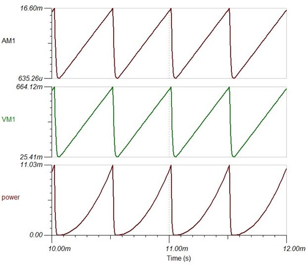
Here's the circuit so far with test meters attached
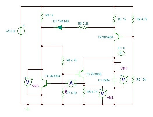
And, here are the waveforms
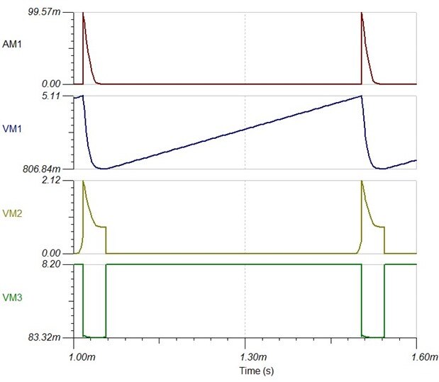
I included an ammeter so that we could see the base current of T4. In this case (220n capacitor)
the peak current is almost 100mA, though it declines quite rapidly. The transistor is heavily
saturated, so the recovery at the end will be slow.
We now have an oscillator generating a sawtooth waveform.
What's the purpose of D1 and R8? At first glance it may look like something being fed back from
the output, but it's actually the other way round. When T4 turns on, D1 conducts and pulls the
emitter of T2 down until it is below the base voltage and T2 turns off. That stops the current
source whilst the discharge takes place. That's to avoid the situation where the discharge partly
completes and then hangs at a point where the charge current matches the discharge current.
The rest of the circuit is simply an emitter follower arranged to buffer the capacitor voltage
without loading that point of the circuit too much. R4, in conjunction with the dc resistance of
the speaker, reduces the output level to something sensible. I've plotted the power at the
speaker by asking the post-processor to multiply AM1 by VM1 - it's just a few milliwatts, so it
will be quite quiet.
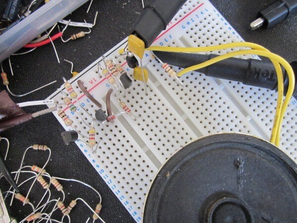
BREADBOARD
So now we've seen how it works, let's build it on a prototyping breadboard to see how well the
real circuit matches the simulation. I couldn't find a 220n, so I've used two 470n in series to
give something roughly similar.
Here it is on the board
and here are the waveforms that the 'scope sees at the top of the capacitor (yellow trace) and
the top of the 4k7 resistor at the collector of T3 (blue trace).
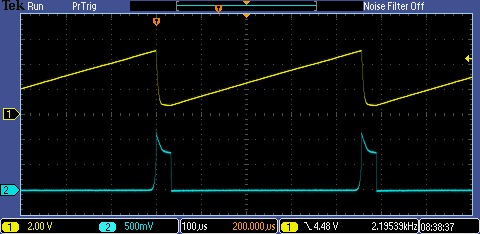
Roughly similar to what we saw with the simulation.
Even with just a few milliwatts of power, the loudspeaker makes an irritating sound -
loud enough that I quickly disconnected it whilst making the 'scope measurements. I'll spare you
the video.
There are several ways the frequency of the output could be changed. Changing the capacitor value
is one way. Alternatively, we could modify the current source either by varying the emitter
resistor or by changing the base voltage given by the potential divider. That then naturally
leads on to the interesting thought that we could disconnect the lower resistor from ground and
drive it with a voltage, which would give us a simple VCO (voltage-controlled oscillator) and suggests
a way we could, perhaps, lock the ramp to another periodic signal.
[1] Application Report: e-line Transistor Applications. Ferranti Semiconductors. 8th Edition.
1975.
Top Comments