


I've been a long time user of the Papilio FPGA board and last year I saw a friend of mine acquire an early prototype of the Pipistrello FPGA board which I found quite intriguing. I've been meaning to get my hands on one and early this year, Magnus Karlsson, the creator of the Pipistrello FPGA board, released an updated design, the Pipistrello rev 2.0. This was just the kick I needed to make me get in touch with him. Since he does not appear to be actively selling these, I emailed him on the off chance he had a spare blank PCB intending to buy the components separately and assemble it myself. He quickly replied mentioning the difficulty of assembling 0402 sized and BGA footprint components. He offered to sell me a fully assembled and tested board and, not being a fool, I jumped at the opportunity. The board arrived in just under a week, USPS international shipping.
Magnus has been kind enough to release all the schematic and design sources of the Pipistrello rev 2.0 board and these can be downloaded from his web site. The board specs are also listed there too.
Click on picture below for high-res.
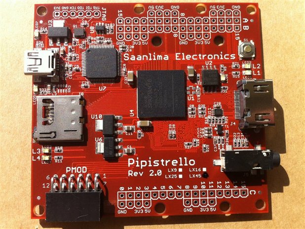
The central feature of the board is the FPGA, it is the same chip used on the Digilent Atlys board, a Xilinx Spartan 6 family LX45 FPGA in a CSG324 package, which is basically a 324 pin BGA package. In terms of performance, it sits squarely in the middle of the Spartan 6 family and it is also the largest FPGA available in the 324 pin BGA package, anything more powerful would require a 484 or larger BGA package. One good thing is that all Spartan 6 family members within a certain package size are pin compatible, so this board could be populated with either a LX25, LX16 or an LX9 in descending performance order and therefore cost, to suit different user budgets. As it stands the LX45 provides the user with well over 43K logic cells, about 400Kbits of distributed RAM, just over 2Mbits of dedicated block RAM and dedicated MCB (memory controller blocks) which allow the user to interface to SDRAM chips without having to code (or even understand) all the complexities and intricacies of driving the SDRAM's bus and performing refreshes.
This brings us to the LPDDR (low power double data rate) also known as Mobile DDR, SDRAM memory chip. This is a 32Mbx16 Micron chip mounted on the opposite side of the board. The LPDDR SDRAM is connected to bank 3 of the FPGA which becomes dedicated to being a SDRAM controller through an MCB. The memory can be clocked at up to 200MHz and since it is a DDR (double data rate) memory that means it can transfer data at 400MHz rate. The data in this instance is 16 bits wide, or 2 bytes at 400MHz giving a theoretical maximum of 800Mbytes/sec dependent of course on the user portion of the design being able to keep data flowing into and out of the controller's pipelines fast enough.
Also attached to the FPGA is a Micron N25Q128 serial Flash memory chip. This is used to store the user design which the FPGA loads and implements at power on allowing the board to have a non volatile persistent design. Since the Flash is 128Mbit in size (16MBytes) and the LX45 bitstream is usually under 2MBytes, this leave significant space in the Flash for user data to be stored. Once the FPGA has loaded its design from the Flash at power on, the Flash can be accessed by the user design and further data retrieved at will. The Flash supports serial, bi and quad access at up to 108MHz with automatic address increment. This means that in quad mode we can stream 4 bits from the Flash at 108MHz for a total rate of 54MBytes/sec for sequential acceess, less for random access as new addresses will need to be loaded reducing the total data rate.
The board features a FT2232H chip which can be seen in the top left corner of the board next to the USB connector. The FT2232H is a high speed (480Mb/s) dual channel USB to UART/FIFO, one of the channels is fully dedicated to the FPGA's JTAG pins and is used to program the board. Both Windows and Linux programming utilities are provided and these can be used to either upload a design to the FPGA only (volatile) or to program the on board Flash memory (non volatile). The other channel of the FT2232H is available to the user design, a total of 13 pins are connected to the FPGA. This can be used as a high speed 8 bit parallel + handshake bus or as an RS232 channel. The official maximum transfer rates are up to 12Mbaud for RS232 and 10Mbyte/sec for parallel FIFO.
The board has a 50MHz crystal oscillator populated on the other side of the board with an extra space left unpopulated on the top of the board (labelled U1) for a second oscillator leaving the user the option to fit a custom frequency crystal oscillator. For the most part this should not be neccessary as the FPGA's internal PLL and DCM modules can generate pretty much any frequency desired from the existing 50MHz.
A standard microSD socket connects all pins directly to the FPGA allowing for large removable storage provided the user has a design implemented that can access the microSD. Such designs have already been written and published on OpenCores.
On the opposite side of the board from the microSD we have an HDMI connector. Again all pins are directly connected to the FPGA including the DDC pins (via a level translator) allowing the FPGA to read the attached monitor's capabilities. As a demo, Magnus flashed a project on the Pipistrello board based on the Xilinx xapp495 that can display test patterns on an HDMI monitor from 640x480 through 1280x1024 in full color. It is of course also possible to output audio through the HDMI connector provided the user design has implemented the appropriate encoding of the audio in the HDMI signal.
Just below the HDMI connector we have a standard 3.5mm stereo audio jack output. This is essentially two pins, each connected to the FPGA via an RC network. This allows the FPGA to generate two independent audio channels via a technique called Sigma Delta modulation explained in the Xilinx xapp154 document.
The board has five user controlled LEDs directly attached to the FPGA, LED1 (green) and LED2 (red) are placed just above the HDMI connector, LED3 (green) and LED4 (red) are just below the microSD slot and the final LED5 (red) is placed above the microSD slot. A single button is located on the board above the HDMI connector. Unlike some other designs this is not a reset button that triggers an FPGA reconfiguration, instead this button simply connects to an FPGA general IO pin and can be used by the user design as a reset signal if desired or just ignored.
Finally a very important feature that makes this a versatile experimenter's board: user IO. The board has a total of 56 available pins for user IO brought out to standard 0.1" headers. These are all 3.3V pins and it would not be advisable to connect them to 5V logic without a level translator, The first connector is a standard dual row Digilent PMOD. Each row provides 4 logic IO pins plus 3.3V power and ground. This means that the user has a large number of existing PMOD board they can just purchase from Digilent and simply plug in and use. Examples of PMODs available are A/D and D/A converters, GPS module, capacitive touch module, WiFi, Bluetooth, LCD modules, joystick, switches, keypads, rotary encoder modules, Network Interface module, the list goes on...
Additionally Magnus chose to put Papilio compatible "wing" connectors. Each wing consists of 8 user IO pins and four power pins, ground, no connect, 3.3V and 5V. Just like the Papilio, on one side two 8 bit wings end to end can form a 16 bit wing and on the other side we have four 8 bit wings that can be two side by side 16bit wings. These all can accept Papilio wings including Papilio Megawings (large board that stacks on top of the FPGA and connects to all wing headers simultaneously). Other than a logical grouping of these IOs into "wings' there is no reason for the user not to treat these as 48 completely independent IO pins and they all can be used without any restriction.
Overall, this looks to me like a well designed experimenter's board that has been very cleanly put together. I haven't asked Magnus but my guess is that this board was professionally assembled with a pick and place machine and proper oven reflow soldering rather than by hand since all the minuscule 0402 sized components are placed spot on in their place without a single one being crooked and they all have just the right amount of solder, not too much, not too little. After using this board for a few days I'm completely satisfied and it was well worth the purchase.
Big thank you to Magnus, not just for creating a great board, but also for openly sharing the design files and schematics. Also big thank you to Jack Gassett from Gadget Factory, the creator of the Papilio FPGA board which was the inspiration behind Pipistrello.
Top Comments